Huawei’s New Chip Strategy Signals Intensifying Battle With Apple and Nvidia

Huawei’s New Chip Strategy Signals Intensifying Battle With Apple and Nvidia
By
Alina Sinclair
Last updated:
May 25, 2026
First Published:
May 25, 2026

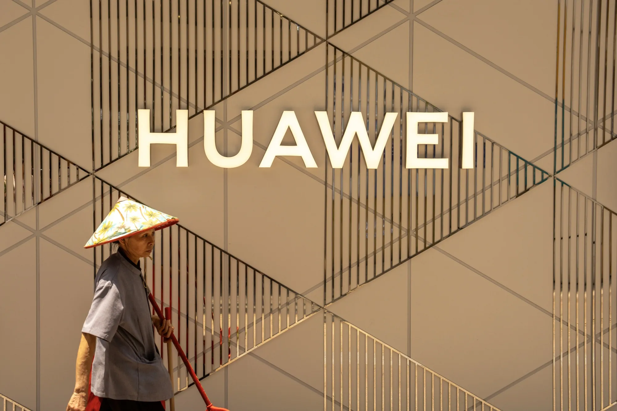
Photo: Bloomberg
Chinese technology powerhouse Huawei has revealed a new semiconductor design strategy that could reshape the company’s future ambitions in smartphones and advanced computing. The company announced that its upcoming Kirin processors, expected to debut later this year, will be the first chips built using a newly developed architecture known as “LogicFolding.”
The announcement arrives at a critical moment for the global technology industry. Competition between Huawei, Nvidia, and Apple is becoming increasingly aggressive, particularly in China, where semiconductor restrictions, artificial intelligence growth, and smartphone market share battles are colliding.
Huawei believes the new architecture can dramatically improve chip efficiency and performance over the next decade. While the company described the technology as a major step forward, analysts remain divided over whether the approach represents a true breakthrough in semiconductor manufacturing or simply an innovative redesign of existing methods.
Huawei Introduces LogicFolding Technology
Huawei says LogicFolding represents a different way of constructing semiconductor systems. Instead of relying solely on traditional chip scaling methods, the approach restructures how chip components communicate and interact internally.
The company claims the architecture expands chip layouts from a single-layer structure into a more advanced multi-layer design. According to Huawei executives, this creates shorter communication pathways between components and allows transistors to interact more efficiently.
The intended result is higher computing performance with lower power consumption.
Tingbo He, president of Huawei's semiconductor business and a director on the company's scientist committee, explained that the architecture creates significantly more interaction points between transistors, improving overall system efficiency.
Industry experts believe such an approach could help offset one of the semiconductor industry's biggest challenges: diminishing returns from traditional scaling methods.
Why This Matters for Nvidia and Apple
Huawei’s latest move extends beyond smartphone technology. It could affect multiple areas of the global technology landscape.
For Nvidia, pressure is growing in the Chinese market. U.S. export restrictions have limited the company's ability to sell some of its most advanced AI processors in China for several years. Those restrictions have opened opportunities for Chinese firms to accelerate domestic alternatives.
Recently, Nvidia CEO Jensen Huang acknowledged that the company had effectively surrendered portions of the Chinese market to Huawei as local technology ecosystems continue expanding.
Analysts suggest Huawei's progress could further narrow Nvidia’s future opportunities in the region.
George Chen, partner and co-chair of digital practice at The Asia Group, said Huawei’s trajectory may reduce the remaining opportunities for advanced AI chip sales in China.
The implications for Apple could also be substantial.
Huawei’s return to the premium smartphone market has already altered competitive dynamics. The launch of the Mate 60 smartphone in 2023 surprised the industry by introducing advanced 5G capability despite ongoing U.S. restrictions.
That launch helped Huawei regain market share in China and intensified pressure on Apple's iPhone business in one of the world's largest consumer markets.
As Huawei strengthens its in-house chip capabilities, competition in premium smartphones may become even more intense.
Huawei’s Long-Term Goal: Reaching Equivalent 1.4-Nanometer Performance
One of the most ambitious claims from Huawei’s presentation involved future processing capabilities.
The company stated that by 2031, its design approach could potentially achieve performance and density equivalent to 1.4-nanometer process technology.
For context, semiconductor manufacturing processes measured in nanometers generally represent increasingly compact and efficient transistor designs. Smaller nodes typically allow higher performance and lower power consumption.
Current global manufacturing leaders are still advancing toward the next generation of chips. Taiwan Semiconductor Manufacturing Company has recently begun large-scale production efforts for 2-nanometer technologies.
Huawei’s projection immediately generated debate among industry observers.
Several analysts questioned whether the company was referring to actual manufacturing capabilities or to performance gains achieved through architectural optimization.
Experts Question the Scale of the Breakthrough
Not everyone in the semiconductor industry is convinced by Huawei’s claims.
Technology specialists argue that design improvements and manufacturing breakthroughs are fundamentally different challenges.
Paul Triolo, head of technology for Asia and the Americas at DGA Group, suggested that folded or stacked chip designs can improve transistor density and efficiency, but they do not automatically solve broader engineering issues.
Some of those challenges include:
• Heat management during heavy processing workloads
• Production consistency and manufacturing yields
• Long-term power efficiency
• Device reliability at advanced scales
• Large-scale manufacturing complexity
Experts note that while architectural innovation can produce meaningful gains, achieving true next-generation manufacturing standards involves overcoming numerous technical barriers simultaneously.
Huawei Wants to Establish a New Semiconductor Principle
Beyond hardware improvements, Huawei also appears to be shaping a broader scientific narrative around its research.
The company introduced what it calls the “Law of Tau,” also referred to as “τ scaling,” positioning it as a framework for future semiconductor development.
For decades, the industry has relied heavily on Moore’s Law, the observation that transistor density on chips roughly doubles every two years while costs decline.
However, many industry leaders have argued that Moore’s Law is becoming increasingly difficult to sustain.
Rather than focusing only on transistor shrinkage, Huawei’s proposed principle emphasizes broader system optimization, including:
• Reducing communication distances inside chips
• Stacking computational logic structures
• Improving memory interaction efficiency
• Integrating chip design with software and packaging systems
• Optimizing computing clusters as unified systems
Industry analysts describe this as a shift from pure manufacturing advancement toward an ecosystem-level engineering strategy.
The Road Ahead Remains Challenging
Despite Huawei’s ambitious vision, company executives acknowledged that the technology remains at the beginning of a long development cycle.
The company described the initiative as a decade-long roadmap rather than an immediate transformation.
Significant engineering hurdles still remain before LogicFolding can mature into large-scale commercial deployment.
Even so, Huawei's latest announcement highlights a broader shift occurring across the semiconductor industry. As traditional scaling methods become harder and more expensive, companies are increasingly searching for alternative pathways to improve performance.
For Huawei, this strategy may become one of the most important technological bets in its effort to strengthen its position against both Apple in smartphones and Nvidia in advanced computing hardware.
.webp)
Popular articles



Subscribe to unlock premium content
Celebrity-Endorsed High-Altitude Vineyards Transform Luxury Wine Market

Liquid Luxury on Ice

Hollywood’s Forgotten Treasures Become the Ultimate Status Symbol

Celebrity-Endorsed High-Altitude Vineyards Transform Luxury Wine Market
Liquid Luxury on Ice
Celebrity-Endorsed High-Altitude Vineyards Transform Luxury Wine Market